SELF |
34 |
|
|
|
|
SELF |
34 |
|
|
|
|
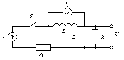
Now let us consider the second equivalent circuit, in which we substitute the contact gap by parasitic capacitance shunted by a resistance RL; its appearance is shown in Fig. 16. |
|
Fig. 16. Equivalent for the contact circuit in which the contact gap is substituted by a parasitic capacitance shunted by a resistance
|
The characteristic equations of this circuit will be |
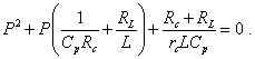 |
(5) |
Oscillation processes will arise in them at the conditions |
| (6) |
Substituting to (6) the values of active resistance of inductance and parasitic capacitance from the above consideration for the circuit in Fig. 15, we will yield |
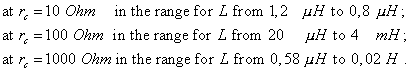 |
(7) |
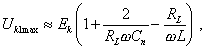
With the circuit shown in Fig. 16 we see another pattern. With considerable shunting of parasitic capacitance, the oscillation process can arise in a very narrow band of inductances, certainly less than usual inductances in contact circuits. Only at shunting resistances closely spaced to that of inductance in our case, the upper level becomes comparable with the load inductance. In the rest of band, in this circuit the aperiodic process will take place, which corresponds to the monotonous charging of parasitic capacitance of the gap. On the basis of this brief analysis, we can conclude the following: - when the contacts were open but shunted by only a parasitic capacitance, there in the circuit arises only an oscillation process; - when the contacts were open but shunted by a parasitic capacitance and a resistance, there in the circuit arises only an aperiodic (monotonous) process. This mathematical analysis corroborates that the monotonous sections of voltage growth can form only in case of contacts shunted by an active resistance, and those surge-like - only in case of lifted shunt, which takes place at the monotonous stage of voltage relaxation. The overvoltage arising at the contacts due to the oscillation process is the more, the more inductance and less capacitance and resistance of the load are. The value of the first maximum of voltage for the circuit shown in Fig. 15 can be determined as |
 |
(8) |
where Uk is the momentary value of the
between-contacts voltage; Ek is the permanent voltage of the feeding
source; Estimating the overvoltage taking place at real values of
parameters Ek = 60 V , Ck = 10 |
Beyond any doubt, a microne-wide contact gap is unable to stand such overvoltage; this means, the gap breakdown has to usually occur at the tops of oscillations, and bright points in these oscillograms correspond to that. Actually, if we suppose that bright points correspond to the amplitude value of the first maximum of transient voltage at the opening contacts, due to falling current of load inductance, they would lay on a descending curve. As opposite to this, in Fig. 8 we see that points lay on the ascending curve and have the spread of amplitude typical for the spread of breakdown of the gap; this proves that the bright points are produced due to the gap breakdowns. The main feature of this spark process is, it is superimposed on the high-frequency oscillation process that already has arisen in the circuit before the gap breakdown. Due to this, an abrupt change of voltage in the circuit disables the discharge to develop fully. Because of it, the affection of spark process onto the voltage change in the circuit is limited by the fact that its impedance becomes nonlinear. This causes a considerable deformation in harmonic pattern of process and at the same time it abruptly increases the frequency of oscillation process. |
Contents: / 23 / 24 / 25 / 26 / 27 / 28 / 29 / 30 / 31 / 32 / 33 / 34 / 35 / 36 / 37 / 38 / 39 / 40 / 41 / 42 / 43 / 44 / 45 /